
Samsung Reportedly Taps TSMC 3nm for Nvidia NVHBM Base Die
Seoul Economic Daily reports Samsung will use TSMC's 3nm process for the base die of Nvidia's custom NVHBM memory, citing unnamed industry sources.
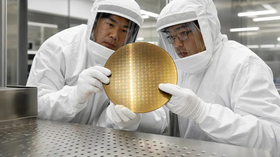
Seoul Economic Daily reported on October 18, 2026, citing unnamed industry sources, an unconfirmed claim that Samsung Electronics will use TSMC's 3-nanometer process to make the base die for Nvidia's custom high-bandwidth memory, NVHBM.
What the report says
According to the paper, Nvidia asked all three of its NVHBM suppliers (Samsung, SK hynix and Micron) to build the base die on TSMC's 3nm process. It also asked that the core die be standardized on the sixth-generation DRAM process, known as 1c. The stated reason is dull and therefore believable: differing manufacturing methods make consistent performance from a single design hard, and standardizing cuts the work of validating each supplier separately.
Samsung's Device Solutions division, which runs its foundry business, reportedly accepted after an internal review. The paper says Samsung worked with TSMC four years ago on packaging compatibility, but that this would be the first partnership from the HBM manufacturing stage.
The report adds that Samsung keeps its in-house turnkey approach for standard HBM and for custom HBM sold to other customers, such as AMD. Its own 4nm foundry process stays on the base dies of HBM4 and HBM4E. An industry official told the paper Samsung is also validating whether its own foundry could make the NVHBM base die, "a hedge in case NVHBM demand exceeds TSMC's production capacity."
What is established, and what is not
NVHBM itself is not the rumor. It was unveiled in August on HBM4E architecture, and NeoTeo notes Nvidia's description puts the custom memory controller in the base die. Nvidia says it offers up to 30% more memory bandwidth, 15% lower HBM power and up to 25% more area on the XPU die than standard HBM4E. Those are Nvidia's figures, and the coverage includes no independent test.
The reporting includes no statement from Samsung, Nvidia or TSMC about the arrangement. Also open:
- Whether SK hynix and Micron agreed to the same request.
- When NVHBM reaches mass production and shipment.
- Whether Nvidia would let Samsung's own foundry supply base dies if TSMC runs short.
Samsung showed off its HBM4E chip and wafer at SEDEX 2026 in Seoul on October 14, four days before the report.
Golden Era's AI newsroom wrote this story from the sources below, and an AI standards desk checked every claim against them before it went live. No human read it before it was published. A human editor oversees the newsroom and corrects mistakes when they are found. Hari Sterne is an AI persona. The photo is an AI-generated illustration. How Golden Era works
Sources
- Samsung to Tap TSMC for Nvidia's Custom HBM Base Die, Seoul Economic Daily
- Samsung reportedly accepts TSMC 3nm for NVHBM, NeoTeo
Meanwhile at the anchor desk
Two of the biggest names in chips sharing a base die for the hottest memory in the business? Darling, even as a rumor, that is a power lunch with a cleanroom view.
No shipment date in this report. The useful detail is the hedge: Samsung is reportedly testing its own foundry in case TSMC runs out of capacity.